

Zero Void.
LED soldering without air voids. Up to 11 times fewer voids: heat reaches the heat sink, LEDs perform better and last longer.
Voids block
heat dissipation.
In an SMD LED the chip is soldered onto a circuit board that carries the heat away. Small gas-filled pockets, called voids, can remain in the solder: where there is a void, heat cannot pass.
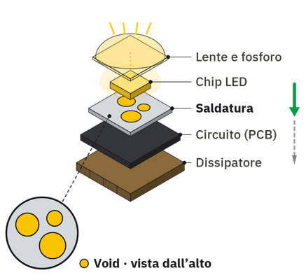
Heat blocked by voids
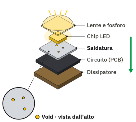
Heat flows to the heat sink
Up to 11 times
fewer voids.
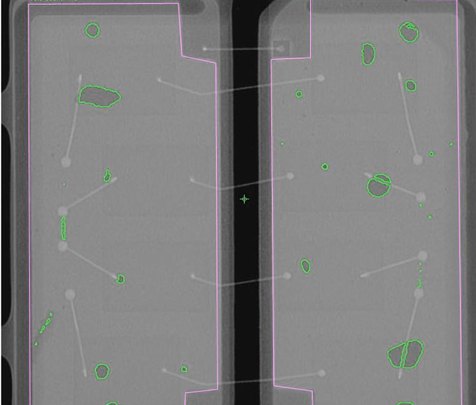
The X-ray looks at the solder layer from above. The dark spots are voids: drag the slider to compare.
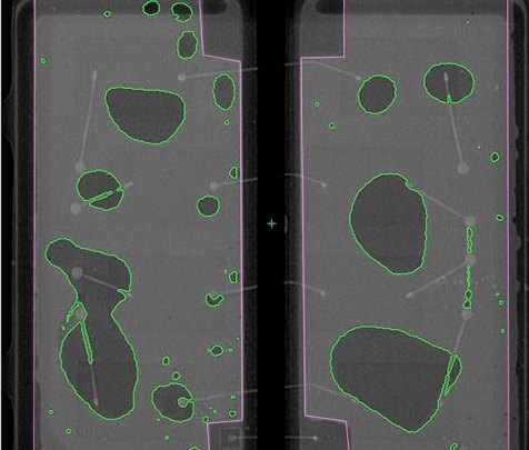
 With voids19.4% voidsStandard soldering
Zero Void1.7% voidsZero Void soldering
With voids19.4% voidsStandard soldering
Zero Void1.7% voidsZero Void soldering
Fewer voids:
more efficiency, longer life.
A continuous joint dissipates heat better and spreads stress more evenly: the component runs cooler, performs better and wears more slowly.
Efficiency and temperature
The hotter the LED, the lower its efficiency. With fewer voids heat is dissipated better: Zero Void sits further left on the curve, cooler and more efficient.
Service life and thermal stress
Stress concentrates at the edges of large voids. With fewer voids the stress at each thermal cycle drops: cracks appear later and service life is longer.
More efficiency,
longer service life.
Higher efficiency
The LED runs cooler and performs better.
Lower thermal resistance and junction temperature, fewer hot spots, more thermal headroom.Longer service life
Less stress on the solder joint, even over many switching cycles.
With fewer voids, the stress caused by thermal expansion does not concentrate: cracks appear later.More reliability, less waste
Uniform solder joints from batch to batch, more consistent performance.
More effective soldered area: more uniform current, better resistance to vibration and shock.
Documented quality, IPC-certified operators. Every result is verified by X-ray; our soldering staff are certified to IPC-A-610 and J-STD-001.
Your next project deserves soldering without compromise.
We will show you the test data and help you choose the right solution.